Research Projects
2D Materials
Complex Oxides
Nanocrystals
TEM/STEM Simulation
Electronic Orbitals
Zeolites
Theory
Equipment
Resources (code)
Research Support
research
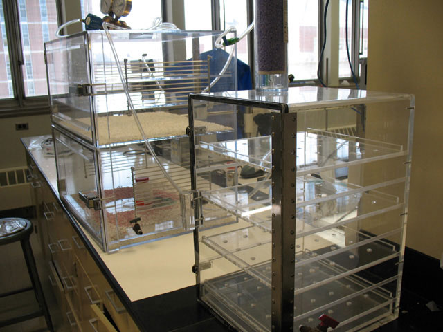
Our Lab (454 Amundson Hall)
Electron Microscopes
Transmission Electron Microscopes
FEI Titan G2 60-300 X-FEG (Scanning) TEM
Monochromated and Aberration-Corrected
Operational at 60, 80, 200, and 300 kV;
Point-to-point resolution of 0.20 nm with information limit of 0.08 nm;
ADF-STEM with resolution of 0.063 nm at 300 keV;
ChemiSTEM EDX spectrometer;
Gatan Enfinium EEL spectrometer with 0.17 eV resolution;
Gatan Ultra1000XP 2k x 2k CCD;
ThermoFisher Talos (coming soon)
Operational at 60, 100, 200 and 300 kV;
Point-point resolution of 0.20 nm with information limit of 0.14 nm;
ADF-STEM with resolution of 0.19 nm;
EDAX rTEM EDX spectrometer;
Gatan Enfina EEL spectrometer;
Gatan UltraScan 2k x 2k CCD;
FEI Tecnai G2 F30 Cryo (Scanning) TEM
Operational at 100, 200 and 300 kV;
Point-point resolution of 0.24 nm with information limit of 0.15 nm;
ADF-STEM with resolution of 0.24 nm;
Gatan UltraScan 4k x 4k CCD;
Gatan GIF 2002 energy filter and EEL spectrometer;
Gatan 692 tv-rate CCD positioned behind GIF;
FEI Tecnai T12 TEM
Operational at 120 kV;
Point-point resolution of 0.34 nm;
Gatan MSC794 1k x 1k CCD;
Gatan 692 tv-rate CCD;
Oxford Inca EDX spectrometer.
TEM Holders
Low-background single- and double-tilt, tilt-rotate;
Single- and double-tilt heating;
Protochips Poseidon Select Liquid Cell;
Hysitron PI95 PicoIndenter;
Cryo and tomography holders;
Protochips Fusion Select Double-tilt Heating;
Scanning Electron Microscopes
JEOL 6500 FEG SEM
Accelerating voltage from 0.5 to 30 kV;
Secondary electron imaging with resolution of 1.5 nm;
Centaurus backscatter detector;
Thermo-Noran Vantage EDX system;
Gatan (Oxford) MonoCL 2 system;
HKL EBSD system;
Samples up to 50x125x125 mm in size.
FEI Helios NanoLab G4 FIB/SEM Dual-Beam
Fastest and easiest preparation of site-specific, ultra-thin high-resolution S/TEM specimens for a wide range of materials;
Final polishing with very low energy ions, enabling the creation of ultra-thin TEM lamella with sub-nm damage layers;
FIB milling resolution of 10 nm;
SEM imaging with resolution of 0.6 nm;
Gallium ion beam & electron dual-beam setup.
Hitachi S-900 (Cryo) Cold FEG SEM
Accelerating voltage from 0.5 to 30 kV;
Secondary e- imaging with resolution of 0.8 nm at 30 kV and 3 nm at 1 kV;
In-lens design allows samples up to 5x10x0.5 mm in size.
Specimen Preparation
Fischione 1010 Ion Mill
Fully programmable and easy to use;
Adjustable rocking angle;
Variable energy milling;
0 to 45 degrees milling angle range;
LN2 specimen cooling.
Fischione 1070 "NanoClean" plasma cleaner
Fully programmable gas flow, power, and time;
Load-locked for fast holder insertion and removable;
Large-sample access door for cleaning of large samples;
Allied MultiPrep Polishing systems
Two MultiPrep systems in Mkhoyan Lab and one in CharFac;
Utilized primarily for preparation of wedge specimens;
Multiple polishing pads and lubricants available;
Copyright 2017 Mkhoyan Lab
151 Amundson Hall, 421 Washington Ave. S.E.
Minneapolis, MN 55455 USA


